
🧪 What is Materials Science & Engineering?
Materials science is the interdisciplinary field that investigates the structure, properties, processing, and performance of materials. Materials engineers design and create new materials with specific properties — stronger, lighter, more conductive, or more durable than existing options. From the steel in skyscrapers to the silicon in computer chips, from carbon fiber in aircraft to biodegradable polymers in medicine, materials science underpins every technological advancement.

🔬 Atomic Structure & Bonding
Materials properties originate at the atomic level. How atoms are arranged and bonded determines whether a material is hard or soft, conductive or insulating, transparent or opaque.
| Bond Type | Characteristics | Examples |
|---|---|---|
| Metallic | Electron sea, ductile, conductive | Iron, copper, aluminum |
| Ionic | High melting point, brittle, insulating | NaCl, ceramics, oxides |
| Covalent | Very strong, directional bonds | Diamond, silicon, polymers |
| Van der Waals | Weak, secondary bonds | Graphite layers, polymers |
Stress = Force / Area | Understanding atomic bonding explains material strength, ductility, and failure mechanisms.
💎 Crystal Structures & Crystallography
Many materials form crystalline structures — atoms arranged in repeating patterns called unit cells. The arrangement determines properties like strength, conductivity, and optical behavior.
| Crystal Structure | Examples | Properties |
|---|---|---|
| Body-Centered Cubic (BCC) | Iron (α), tungsten, chromium | Strong, less ductile |
| Face-Centered Cubic (FCC) | Aluminum, copper, nickel, gold | Ductile, formable |
| Hexagonal Close-Packed (HCP) | Magnesium, titanium, zinc | Anisotropic properties |

📦 Four Major Material Classes
1. Metals
Metals are characterized by metallic bonding — a sea of delocalized electrons. This gives them high electrical and thermal conductivity, ductility (ability to deform without breaking), and strength. Applications: structural components, wiring, transportation, tools.
2. Ceramics
Ceramics are compounds of metallic and non-metallic elements, typically oxides, carbides, or nitrides. They are hard, brittle, heat-resistant, and chemically stable. Applications: refractories (furnace linings), cutting tools, electronics substrates, bone implants.
3. Polymers
Polymers are long chains of repeating molecular units (monomers). They are lightweight, corrosion-resistant, and easily processed. Applications: packaging, medical devices, textiles, automotive parts, electronics housings.
# Polymer Structure Types:
Linear Polymers: Chains connected end-to-end (polyethylene)
Branched Polymers: Side chains off main chain
Cross-linked Polymers: Chains connected at multiple points (rubbers, epoxies)
Thermoplastics: Soften with heat, reversible (PET, PVC, polypropylene)
Thermosets: Permanent cross-links, cannot be remelted (epoxy, phenolic)
4. Composites
Composites combine two or more materials to achieve properties impossible with individual components. Reinforcement provides strength; matrix binds and protects. Examples: fiberglass (glass fibers + polymer), carbon fiber composites (carbon fibers + epoxy), concrete (aggregate + cement).
🔬 Nanotechnology: The Science of the Very Small
Nanotechnology manipulates matter at the atomic and molecular scale — typically 1 to 100 nanometers. At this scale, materials exhibit unique quantum effects and dramatically different properties than their bulk counterparts. 1 nanometer = 1 billionth of a meter (about 10,000 times smaller than a human hair).
⚫ Revolutionary Carbon Nanomaterials
| Material | Structure | Properties | Applications |
|---|---|---|---|
| Graphene | Single atomic layer of carbon in honeycomb lattice | Strongest material known (200x steel), highly conductive, transparent | Flexible electronics, batteries, composites, sensors |
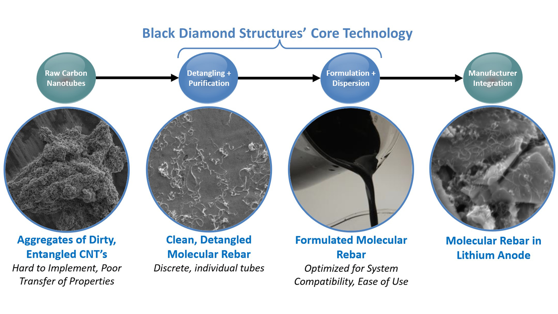
| Carbon Nanotubes (CNT) | Rolled graphene sheets (single or multi-wall) | Exceptional strength, thermal conductivity, electrical properties | Structural composites, nanoelectronics, drug delivery |
| Fullerenes (Buckyballs) | C60 molecules shaped like soccer balls | High electron affinity, lubricating properties | Lubricants, antioxidants, drug delivery |
🧬 Nanoparticle & Nanomaterial Types
- Quantum Dots: Semiconductor nanocrystals (2-10 nm) that emit precise colors. Used in displays, biological imaging, solar cells.
- Metal Nanoparticles: Silver nanoparticles (antibacterial coatings), gold nanoparticles (diagnostics, drug delivery), platinum nanoparticles (catalysts).
- Nanowires & Nanorods: One-dimensional structures for nanoelectronics, sensors, and energy devices.
- Nanolayers & Thin Films: Atomic layer deposition creates coatings with precise thickness for electronics, optics, and barriers.
- Nanoporous Materials: Metal-organic frameworks (MOFs), zeolites — high surface area for gas storage, catalysis, filtration.
🔍 How Scientists See Atoms
Understanding materials at the nanoscale requires powerful characterization tools:
- Scanning Electron Microscopy (SEM): High-resolution imaging of surfaces (resolution ~1 nm). Used for morphology, fracture analysis, particle sizing.
- Transmission Electron Microscopy (TEM): Atomic-resolution imaging, crystal structure determination (resolution ~0.1 nm).
- Atomic Force Microscopy (AFM): Surface topography at atomic scale, measures forces between tip and sample.
- X-Ray Diffraction (XRD): Determines crystal structure, phase identification, lattice parameters.
- Spectroscopy: Raman, FTIR, XPS identify chemical composition and bonding.
🏭 Processing & Manufacturing Methods
| Process | Description | Applications |
|---|---|---|
| Additive Manufacturing (3D Printing) | Layer-by-layer fabrication from digital models | Prototyping, custom implants, aerospace components |
| Chemical Vapor Deposition (CVD) | Gas-phase reactions deposit thin films | Semiconductors, graphene, coatings |
| Electrospinning | Electric field draws polymer fibers (nanometers to microns) | Tissue scaffolds, filtration membranes |
| Sol-Gel Processing | Solution to gel to ceramic transformations | Optical coatings, nanoparticles, aerogels |
| Mechanical Alloying | High-energy ball milling creates nanocomposites | High-strength alloys, metal matrix composites |
🏥 Nanomedicine & Biomedical Applications
Nanotechnology is revolutionizing medicine with targeted drug delivery, improved diagnostics, and regenerative therapies.
- Targeted Drug Delivery: Nanoparticles functionalized with antibodies deliver chemotherapy directly to tumors, reducing side effects.
- Contrast Agents: Iron oxide nanoparticles enhance MRI contrast for better cancer detection.
- Antimicrobial Coatings: Silver nanoparticles in wound dressings prevent infection.
- Tissue Engineering: Nanofiber scaffolds guide cell growth for tissue regeneration.
- Biosensors: Gold nanoparticles enable rapid disease detection (lateral flow tests).
- Artificial Implants: Nanostructured surfaces improve osseointegration of hip and dental implants.

🔋 Energy Materials & Nanotechnology
- Batteries: Nanostructured anodes (silicon nanowires) increase lithium-ion capacity 10x. Solid-state electrolytes enable safer, higher-density batteries.
- Supercapacitors: Graphene and carbon nanotube electrodes provide rapid charge/discharge for energy storage.
- Solar Cells: Perovskite solar cells (efficiency >25%), quantum dot solar cells, and dye-sensitized cells offer low-cost alternatives to silicon.
- Fuel Cells: Platinum nanoparticles catalyze hydrogen reactions. Nanostructured membranes improve efficiency.
- Catalysis: Nanocatalysts enable cleaner chemical processes, hydrogen production, and emission control.
💻 Nanoelectronics & Quantum Computing
The semiconductor industry has driven miniaturization for decades. Current transistors are ~5 nm — approaching atomic scales.
- Moore's Law: Transistor density doubles approximately every 2 years, enabled by materials innovations.
- 2D Materials: Beyond silicon — transition metal dichalcogenides (TMDs) for next-generation transistors.
- Spintronics: Uses electron spin (not just charge) for information processing — magnetic tunnel junctions, MRAM.
- Quantum Computing: Qubits require extreme isolation. Superconducting circuits, trapped ions, and silicon quantum dots are leading approaches.
- Flexible Electronics: Organic semiconductors, graphene, and nanomaterials enable bendable displays and wearable sensors.
🌍 Sustainable Materials & Environmental Remediation
- Water Purification: Nanofiltration membranes remove contaminants, desalinate seawater. Photocatalytic nanoparticles (TiO₂) degrade pollutants.
- Air Filtration: Electrospun nanofibers capture particulates and pathogens.
- Carbon Capture: Metal-organic frameworks (MOFs) absorb CO₂ with high selectivity.
- Biodegradable Polymers: PLA (polylactic acid) from corn starch replaces petroleum-based plastics.
- Self-Healing Materials: Microcapsules release healing agents when cracks form, extending material life.
🎓 Careers in Materials Science & Nanotechnology
| Role | Typical Work | Salary Range |
|---|---|---|
| Materials Scientist | R&D of new materials, characterization | $80-130k |
| Process Engineer | Manufacturing optimization, quality control | $75-115k |
| Nanotechnology Researcher | Academic/industrial research, synthesis | $70-120k |
| Semiconductor Engineer | Chip fabrication, lithography | $85-140k |
| Biomaterials Engineer | Medical devices, implants, drug delivery | $80-125k |